Semiconductor Manufacturing Process – Steps, Technology, Flow Chart
Learn about the essential semiconductor manufacturing process – wafer manufacturing, oxidation, photolithography, etching, deposition and ion implementation, metal wiring, Eds and packaging.
In this article, we will learn about the essential semiconductor manufacturing process. In one of my earlier article, I have already explained about uses of silicon in electronics, which is the main material used to make semiconductors.
In order for silicon to turn into a semiconductor chip, it needs to go through the several complex process of wafer manufacturing, oxidation, photolithography, etching, deposition and ion implementation, metal wiring, Eds and packaging.
Let’s take a closer look at this essential semiconductor manufacturing process.

Table of Contents:
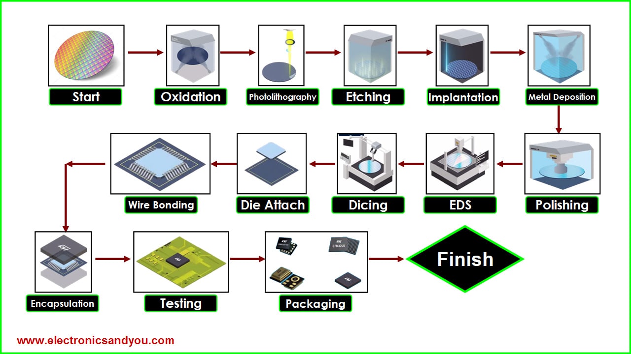
Semiconductor Manufacturing Processes – Steps Involved
| Step# | Process | What Happens |
| 1. | Wafer | Foundation for Semiconductor. |
| 2. | Oxidation | Create Oxide Film on Wafer Surface. |
| 3. | Photolithography | Draw Circuit Design on Wafer. |
| 4. | Etching | Remove Unnecessary Materials. |
| 5. | Deposition and ion implementation | Coating thin film at a desired molecular or atomic level onto a wafer. |
| 6. | Metal wiring | Allows electricity to flow by depositing a thin metal film. |
| 7. | EDS | Process of testing to ensure flawless semiconductor chips. |
| 8. | Packaging | Final wafer are cut into individual semiconductor chips. |
Semiconductor Manufacturing Process – Steps and Technology Used
Let us now understand all of the above steps in detail.
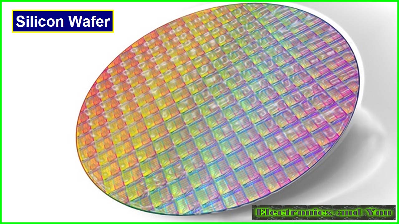
1. Silicon Wafer Manufacturing – The Foundation for all Semiconductor
Semiconductors are stacked high and solid to form a complex structure similar to a high-rise building. Constructing a building starts with the foundation. Similarly, a silicon wafer is the foundation for the semiconductor.
Most wafers are made of silicon extracted from sand. But have you ever wondered how can these tiny grains of sand become a wafer? Here are the steps involved:
- First, sand is heated until it melts into a high purity liquid and then gets solidified by crystallization.
- The resultant silicon rod is called an ingot. These ingots are sliced into a disc thinly sliced wafers.
- The surface of sliced wafers is rough and contains defects. So polishing machines are used to polish the surface of the wafer. The reason is that defects on the surface could negatively affect the precision of an electronic circuit.
- If you look at a photo of a silicon wafers, you can see a grid pattern on the surface.
A wafer made this way is the main material for semiconductors. The larger the diameter of a wafer is, the greater the number of chips that can be produced.
 PS: Silicon is extracted from Silica sand, also known as quartz sand, white sand, or industrial sand. It is made up of: silica and oxygen (SiO2).
I hope now you have learnt about the crystallization process and how does crystallization (solidification) work.
Check:
2. Oxidation – Create Oxide Film on Wafer Surface.
The silicon wafer manufactured in step 1 is not yet conductive. It has to go through a process to make the wafers semiconductive.
First, wafers go through the oxidation process. Oxygen or water vapor is sprayed on the wafer surface to form a uniform oxide film.

This oxide film protects the wafer surface during the subsequent processes and also blocks current leakage between circuits. The film acts as a strong protective shield.
Now the foundation for semiconductor is ready.
I hope this clarifies the thermal oxidation of silicon and difference between dry and wet oxidation process.
Check:
3. Photolithography – Draw Circuit Design on Wafer
Next step is to draw a circuit design onto a wafer which is called the photolithography process. It is also called “photo” for short because it is similar to developing a photo taken on a film camera with semiconductors.
A photo mask functions as the film. A photo mask is a glass substrate with a computer designed circuit pattern.

In order to draw the circuit on the wafer, the photoresist, a material that responds to light is applied thinly and evenly on the oxide film previously placed on the wafer.
Now, when light transfers the patterned photo mask, the circuit is drawn on the wafer surface. Just like developing a photo, a circuit pattern is imprinted on the wafer by spraying, developer and removing unlit areas from the areas that are exposed to light.
After an inspection of the wafer to check whether the pattern is drawn well, it moves on to the next step.
I hope the photolithography printing process is clear to you now.
Check:
4. Etching – Remove Unnecessary Materials
Now it is time to remove unnecessary materials from the wafer surface so that only the design pattern remains.
This is done using a liquid or gas etching technique. All unnecessary materials are selectively removed to draw the desired design.
- Wet Etching: When chemical solutions are used for etching, it is called wet etching.
- Dry Etching: When gas or plasma is used, it is called dry etching.

Let’s imagine constructing a building on a semiconductor chip smaller than a fingernail and thinner than a sheet of paper.
The photolithography process and the etching process are repeated several times on the wafer layer by layer. Here, an insulating film that separates and protects the stacked circuits is required. It is called a thin film. The process is very similar to manufacturing a Multilayer PCB.
5. Deposition and Ion Implementation (Ion implantation)
Coating the thin film at a desired molecular or atomic level onto a wafer is called deposition. Since the coating is so thin, precise and sophisticated technology is required to uniformly apply the thin film on a wafer to give the semiconductor electrical characteristics. Ion implementation / Ion implantation is also required.
A semiconductor made of silicon does not conduct electricity but adding impurities. It conducts current and has conductive properties.

In summary, through the wafer manufacturing, oxidation, photolithography, etching, deposition and ion implementation processes the wafer becomes conductive and numerous circuits are drawn on it.
6. Metal Wiring
Now, in order for this circuit to work, an electrical signal must be applied. It is necessary to create a path for electricity to pass through according to the circuit pattern. This process is called the metal wiring process.
It is a process that allows electricity to flow by depositing a thin metal film using materials such as aluminum, titanium or tungsten so that electricity can pass through the semiconductor wells.

PS:
- Though Copper conducts electricity with about 40 percent less resistance than aluminum, it is avoided in the semiconductor manufacturing process.
- Copper is considered as semiconductor killer. It rapidly diffuses into silicon and changes its’ electrical properties that can prevent the transistors from functioning.
- Aluminum is the most common material for metal interconnects in semiconductor chips. This metal adheres well to the oxide layer (silicon dioxide) and is easily workable.
7. EDS – Energy Dispersive Spectroscopy
The next step is EDS. This is the process of testing to ensure flawless semiconductor chips. In other words, it is a testing step to sort out defective chips.
Yield is a percentage of prime chips relative to the maximum chip count on a single wafer.
The semiconductor chips selected through the EDS process are made in a form suitable for devices.
8. Packaging
This is the last process, the packaging process. The wafer completed through the previous steps are cut into individual semiconductor chips that can be loaded on an electronic semiconductor device.
An individual chip must have a path to exchange electrical signals with the outside and have a form to protect it from various external elements.
The wafer is cut into individual chips and the diced or saw chips are placed on the PCB board.
In the bonding step, the contact point of the semiconductor chip placed on a substrate is connected with the contact point of the substrate. Then molding finishes the chip package to its desired shape.
After final test, sealing and labeling the product name, the semiconductor chip we commonly see is completed.
Semiconductor Manufacturing Process Flow Chart
Video: Semiconductor Manufacturing Process
FAQs: Semiconductor Manufacturing Process
How are semiconductors manufactured?
Following steps are involved in semiconductor manufacturing:
- Wafer Manufacturing
- Oxidation
- Photolithography
- Etching
- Deposition and ion implementation
- Metal wiring
- EDS
- Packaging
What is required for semiconductor manufacturing?
Basic materials required for semiconductor manufacturing are:
- Silicon Wafer
- High-purity water
- hydrocarbon polymers for Photolithography
- Etching Chemicals or Plasma
- Aluminum for Metal Wiring
What is the basic process of semiconductor?
Basic process of semiconductor are: Wafer manufacturing, oxidation, photolithography, etching, deposition and ion implementation, metal wiring, EDS and Packaging.
Semiconductor manufacturing Machine
Following are some of the essential machines required for semiconductor manufacturing:
- Dicing Machine: To cut wafers into individual semiconductor chips with blades.
- Laser Dicing Machine: Uses lasers instead of blades.
- Probing Machine: To perform electrical tests.
- Polish Grinders: To Polish and other applications.
- CMP Machine: To remove unevenness on wafer surfaces.
- Wafer edge grinding Machine.
- Sliced Wafer Demounting and Cleaning Machine
Conclusion
In this article, we learnt about the essential Semiconductor Manufacturing Process.
These complex processes can be separated into the preprocess up to the wafer processing stage and the Post Process, which contains the testing and packaging processes.
We hope you now have a better understanding of how a semiconductor chip is manufactured.
Please SHARE this Article with others. Thanks!
Related Posts:
- Top 10 Semiconductor Manufacturing Companies in India
- TSMC India
- SMT Surface Mount Technology
- SMD Surface Mount Electronic Components for SMT
- Top 10 Largest Semiconductor Companies in the World
- Cleanroom Basics in Manufacturing or Scientific Research
- Electronic Components, Parts and Their Function
- Different Types of Printed Circuit Board (PCB)
- Integrated Circuit (IC) – IC Basic Tutorial
- Soldering in Electronics
- SMT Manufacturing Line and Assembly Process
- Top 5 Green Hydrogen Energy Companies in India Listed in Stock Market
- Surface Mount Transistor
- Types of Electric Circuit


A “Pick & Place Machine” is a piece of industrial equipment used in manufacturing, particularly in electronics assembly and printed circuit board (PCB) assembly processes. Its primary function is to automatically pick up electronic components (such as resistors, capacitors, integrated circuits, or LEDs) from a tray or reel and accurately place them onto a PCB with precision and speed.